Design of Ham Vacuum Tube Transmitters
Vacuum Tube Transmitter
Designs
Power Supply discussion
A few basic guidelines should be followed even in simple minimal-component
vacuum tube transmitters.
Common Point and Bypassing
The vacuum tube “pulls” on the high voltage like a variable resistor. The path
for that “pull” is from cathode to anode, the grids just control the
instantaneous resistance of that path. You can read more about how a tube (or
transistor) drives a tank circuit on this
page.
Because of the tube acting like a
variable resistance in series with the tank input, the RF current’s tube path
is as follows:
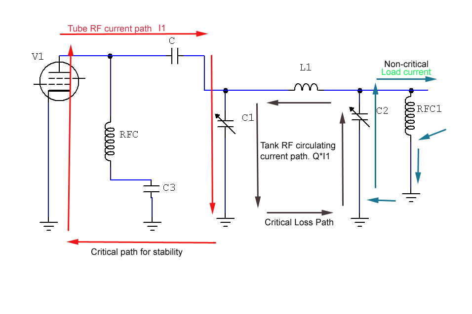
The PA tube cathode, unless intentionally
floated at radio frequencies for RF drive or for RF feedback, should be solidly
bypassed to a low impedance ground plane or a common point shared by C1 (the tank resonating or tuning
capacitor). The red color path above should have minimum uncontrolled impedance,
which means a layout with shortest possible and lowest impedance leads,
including though ground.
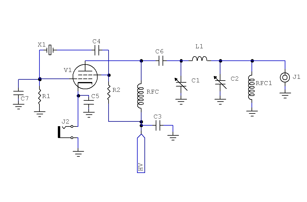
A typical power oscillator (PO)
minimalist single tube transmitter of reasonably good compromise between
complexity, cleanliness, repeatability, and reliability would have every
component serve some critical function. The circuit in Colpitts (tapped
capacitance) or Clapp (modified Colpitts) oscillator form, a reasonable
circuit for PO use, would look
like this:
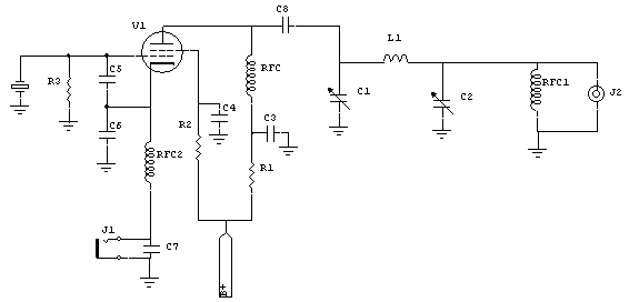
Critical tube path
is:
We see the RF output current conversion from the DC supply is
primarily through C6, back to C1 and C8 through the tube.
Oscillators
Component Function Power Oscillator Colpitts (or Clapp)
R3 sets the oscillating bias voltage developed by grid current. This tube
has zero grid bias unless oscillating. If the tube is not oscillating,
depending on screen and plate voltage, and if the cathode circuit is closed,
the tube can exceed rated anode dissipation. Some fixed bias, either cathode
or grid, would solve this issue. This circuit assumes damage from lack of
oscillation is never a worry. If the tube is protective biased, it has to be
biased at a safe dissipation but must not be near cutoff. If fixed bias is
near cutoff the stage might not oscillate. R3 has a large effect on output
power and crystal current. R3 is typically sized in the many ten’s of
thousands of ohms, somewhere between 47k and 470k is typical. Less
resistance is generally more power at the expense of crystal instabilitly
and more sensitivity to loading and tuning.
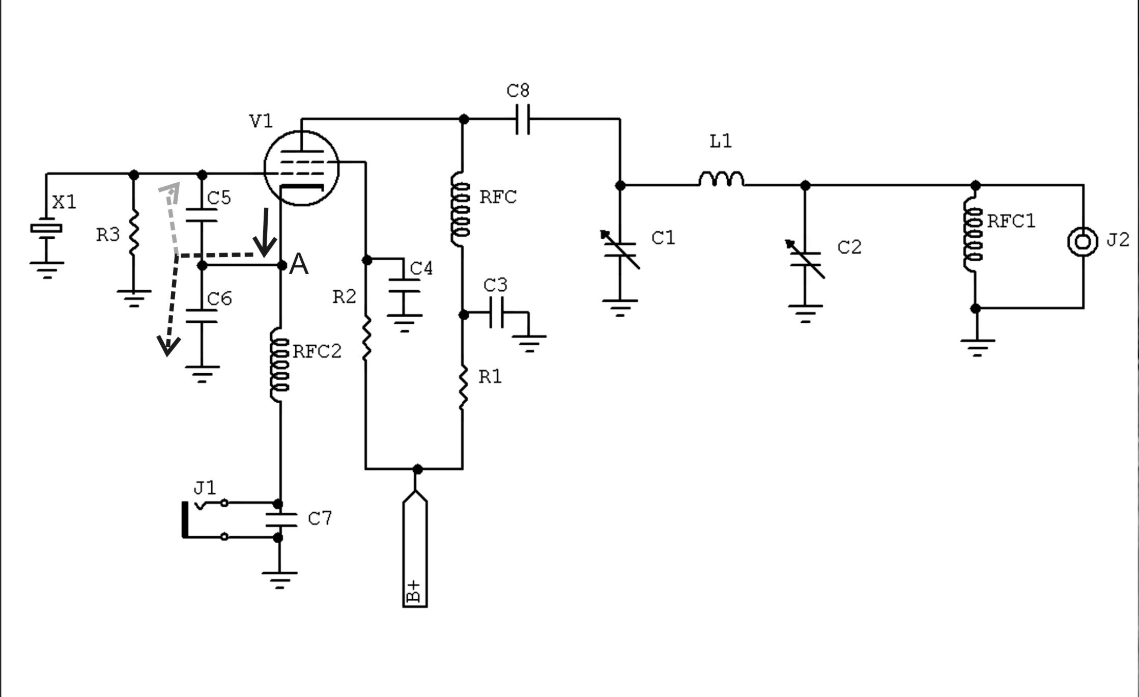
C6 sets cathode RF voltage at point A for a given frequency range and tube cathode
current. This capacitor should be as large as possible while still allowing
oscillation on the highest band with the most sluggish crystal. This cap has
the largest effect on crystal current and least effect on frequency.
C5
limits current into the grid on the positive half cycle and shifts phase in
conjunction with the crystal. C5 should be the lowest value possible while still
allowing oscillation on the lowest frequency with the most sluggish crystal.
It also has a large effect on crystal frequency as it is made smaller.
C6 (and to some extent C5) has a large effect on crystal current, but R3 ultimately
limits oscillator power since it controls tube operating bias and peak currents.
The voltage of all grid and cathode side capacitors should be at least the
dc anode voltage, otherwise a tube fault or open key can damage these
components. C5 is the least critical for voltage.
C4 is the screen
bypass. It should have a low impedance to the ground end of both C6 and C1.
A .001 to .01 uF ceramic disk of more than twice the dc supply voltage is
good enough.
C3 is non-critical and has minimal current. C3 along
with R1 form a low pass filter, reducing RF flowing back to the power
supply.
C8 is a coupling (dc blocking) capacitor. It keeps dc voltage out of the
tank circuit. In most cases almost any value over a few dozen pF will work
the same! The voltage rating and quality is important. This capacitor along
with RFC1 protects your life, so make sure the voltage rating and quality is
good. A 1kV ceramic disc of fairly large physical size, like a typical .01uF
1kV disk, is good.
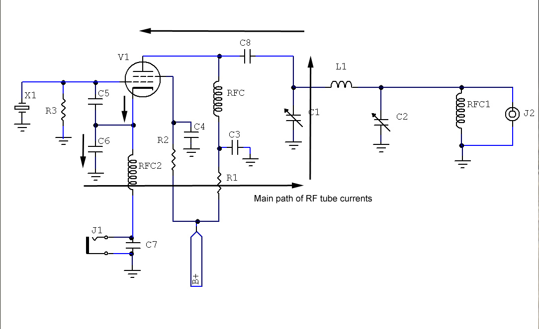
Pierce Power Oscillator (PPO)
In the circuit above, the high current RF tube path is in a loop from C1
andC6, through the tube anode-cathode resistance, through C5, to the
bottom of C1. The tank circulating currents are through C1, L1, C2, and back
through ground to C1. The tank path, C1-L1-C2 and back to C1 ground is by
far the highest RF current path.
R1 sets grid bias by Ig * R1 = Eg1. Bias determines tube power for a
given screen and plate voltage, so it naturally has a large effect on
crystal current.
C7 along with R2 determines crystal current. There is quite a bit of
interaction between components, and some small shunt capacitance from screen
to ground is sometimes needed to allow R2 to be in a safe range for the
tube.
C5 must be at the tube pin to groundplane or common point, the path from
cathode to C1 ground has to be fairly low impedance.
C4 is just blocking, and can actually be a fairly low capacitance value.
It does not hurt to have a resistance, even very high value (millions of
ohms) across the crystal to keep any dc charge off the crystal.
Vacuum Tube Transmitter
Designs
Power Supplies
Power supplies are first, because everything depends on them. A
transmitter’s cleanliness and operating consistency can only be as good as
the power supply permits.
Old power supplies were often not that good. Most supplies used filter
chokes, which can be a very good thing with high vacuum rectifiers (reducing
peak current). Unfortunately, input chokes were often the wrong size for the
bleeder current, making regulation and peak currents worse than not even
using a choke! There is nothing worse than carefully following a recipe and
seeking out specific parts, just to have disastrous voltage regulation when
done.
The primary advantage of a choke input filter is reduction of peak
currents. By virtue of energy storage and release, a properly-sized choke
provides a smoothly changing voltage boost throughout the low voltage part
of the supply sine wave. Conversely, the same choke provides a bucking
voltage near peaks. The mechanism behind this voltage bucking or boosting is
an inductor’s tendency to readjust voltages across the inductor as it tries
to maintain constant current.
A properly sized input choke causes the rectifier to draw
current throughout the entire conduction period of the input cycle. This
current smoothing, almost appearing as a resistive load, extends in a closed
loop from power mains all the way through the power transformer, rectifier
system, and the first filter capacitor.
Capacitor input supplies can be very good for regulation, if high
peak currents are properly dealt with. The only significant
operational problems with higher power capacitor input supplies are caused
by high peak currents, even while average currents are about the same as a
choke input supply. A capacitor input supply draws all of the supply energy
in a short period at the rising edge and just over the crest of each power
line cycle. These high peak currents cause abnormal heating as they increase
voltage drop in components. Capacitor input supplies can be particularly
tough on vacuum tubes, and on old transformers using smaller copper sizes.
To handle the apparent power factor (APF) of heavy charging currents at the
leading edge of each sine wave voltage peak, capacitor input supplies should
use a little larger copper winding size. The capacitor input supply, in
essence, runs only on line voltage peaks. All load power is “taken off the
peaks”. This actually can flatten the peak of the line sine wave, causing
line voltage to measure almost normal on meters even while the mains are
sagging on peaks.
An example of a good power supply is in the AL1200 (AL12 series) power
supplies. I specifically designed the transformer for very tight coupling
with minimal flux leakage, and the largest possible copper size that would
fit in the core window. Because of the low ESR transformer, peak current is
often limited just by the ESR of the power mains. With a really stiff mains,
the AL12 series will hold voltage within 10% from no load to full load. The
price for this voltage stability is very high peak current. I’ve measured
about 40-50 amps peak current at the repeating line sine wave voltage crest
leading edges, while average current over the entire cycle is only about 12
amps. This high peak-to-average current ratio clearly calls for increased
copper size throughout the primary system. Capacitor input designs must
minimize series resistance, or regulation falls apart.
In comparison, a well-designed choke input supply (with properly sized
choke) has an APF (apparent power factor) of nearly unity. Current is drawn
in smooth step with voltage over the entire sine wave, even the descending
slope of the waveform! The smooth current window allows energy to be
extracted from the mains over the entire cycle. This allows much smaller
copper sizes, since the choke input supply requires far less attention to
transformer and power line ESR (equivalent series resistance). With a
properly sized input choke and good components, the power supply’s line
loading appears as a pure resistance.
The bottom line on this is the user has two choices:
1.) Live with the high currents, while maintaining good life and good
regulation, by using low ESR (equivalent series resistance)
transformers, solid state rectifiers, and higher value filter
capacitors2.) Use a properly designed choke input with higher ESR
components. “Properly designed” is the key here, and
proper design requires a critical minimum choke inductance
for the supply’s load impedance under all operating loads
As a closing thought, we often try to correct design issues through power
wasting in bleeder resistors. A low bleeder resistance decreases the ratio
between no load and full load current. If, for example, we waste as
much power in the bleeder as transmitter power demand changes from zero load
to full load, we now have a load change of 50%. We halve the load change as
a percentage, so we might double regulation in a system by wasting power. A
better solution might be to use a better initial circuit design, or the
correct components, so we need minimal wasted power (heat).
By the way, a 50 watt bleeder dissipating 20 watts contributes just as
much heat to the cabinet inside as a 25 watt resistor dissipating 20 watts.
The BTU/hr is exactly the same. X watts of heat will be X watts of
cabinet temperature rise. The higher power component will be physically
larger and run at less temperature, but the heat output will be exactly the
same. The cabinet temperature will rise exactly the same amount for the same
actual power being dissipated, so oversized resistors will not make “the box
around them” cooler.
General Advice on Supplies
When using a vacuum tube rectifier in a transmitter with widely varying
load currents, a choke input filter with proper rating choke
will be the superior system. If solid state parts are an option, a capacitor
input supply is a much better choice for size, cost, and weight.
The required choke inductance is surprising, it will be pretty large. At
120 Hz (60 Hz and full wave rectifier), minimum bleeder current in
milliamperes should be well over E/L. With 700 volts and 5 henries,
the bleeder should draw well over 700/5 = 140 mA.
Another factor is voltage ringing or bounce caused by the choke
inductance and filter capacitance. This “bounce” can result in wild but slow
gyrations in supply voltage at a syllabic rate in a SSB transmitter of class
B modulator, or at a code character rate using CW. This bounce is
minimized using an excessively large value of filter capacitance and minimal
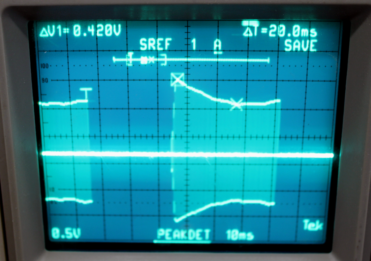
inductance. Here is a screen shot of power supply bounce in my Viking
Valiant when sending a string of dots. The bounce is caused by the filter
choke’s less than ideal load response. It is not caused by the supply being
“weak”. The supply is actually quite good. The scale is 100 volts per
division, peak-to-peak bounce is around 200 volts:
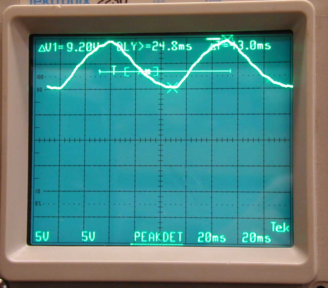 fig.
fig.
1
Unless there is some particular reason to avoid solid state rectifiers,
or unless APF is critical, solid state rectifiers followed by a capacitor
input supply are a much more stable solution. If load current
dramatically varies, like in a CW transmitter, it is probably best to
completely avoid using a filter choke (even in a pi type supply filter).
Contrary to old outdated opinions, transformers and components will live
just fine in a capacitor input supply. The exception would be where
tube-type rectifiers are used. While regulation will not be perfect, a solid
state capacitor input supply’s regulation will typically be far better than
a poorly planned or crudely implemented choke supply. Expect 10% regulation,
or better, from a well-designed capacitor input supply. A choke supply is
much more expensive and heavy, and will be about the same if you are
careful. If the designer or builder is not careful, a choke input supply can
easily have 40% voltage sag!
There are an abundance of bad power supply designs in Handbooks, Ham
transmitters, and articles! Some are beyond bad, and should only be
classified as “terrible”.
A well-designed choke input supply with proper bleeder current outputs
about .9 times the RMS voltage of a transformer, while a capacitor input
supply with solid state rectifier outputs around 1.4 times. Keep this in
mind while selecting a transformer. Also remember, most rectifier tubes have
a pretty high internal impedance. Most rectifier tubes do not “go well” with
high power capacitor input supplies. If you really want to run a tube type
rectifier, the performance problems and complexity of a choke input supply
might become a necessity.
Dual Voltage Supply with Bias
A center tapped transformer can be used to supply stable PA HV and
screen, as well as a lower voltage for early stages. The construction method
below acts as a full wave CT supply for low voltage, and as FW bridge
supply for HV. This system allows equal voltage capacitors without the usual
equalizing worries. Because the capacitors are fixed in voltage division,
capacitors do not need to be the same value. The low voltage supply can have
more capacitance, better suiting increased filter requirements of sensitive,
low-level, stages like oscillators and screen grids. This much better
for voltage stability, and it produces less heat, than the common method of
creating low voltage supplies through large dropping resistors from the full
high voltage.
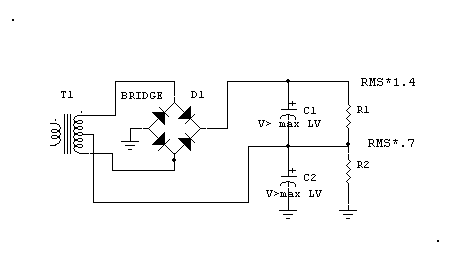 fig
fig
2
This supply, with an appropriate size 500 Vrms center tapped transformer,
would make a pretty good 700V / 350V transmitter supply for 6146’s, 807’s,
and similar tubes. It is simple, easy to build, and lacks complications of
choke input supplies. It provides a very stable “half-voltage” source.
Bias voltages can be derived from a separate winding, a rectifier
negative lead filter choke, or from a very small “backwards” transformer
boosting tube filament voltage. A 120 to 24 volt transformer, for example,
makes a cheap safe 6.3 to 30 volt AC (50 Vdc bias) supply. Bias supplies are
unique, in that a class AB2, B2
or class C tube pushes grid current back into the bias supply. The bias
supply below is derived by boosting the filament through a backwards through
a very small transformer, although conventional transformer could be used.
Resistor R4 must draw several times the grid current expected in the biased
stage(s) to ensure relatively stable bias voltage. R4 could be a slider
resistor with multiple taps, or split into two or three resistors, to
provide several bias voltages. At 4.7k
Expanding on this a bit more:
VR Tube Design
VR (voltage regulator) tubes are not like Zeners. VR tubes have an
ignition or starting voltage, a maximum and minimum current, and a running
voltage. The tube must be held within those ratings during operation, or it
can do some very unusual or unexpected things.
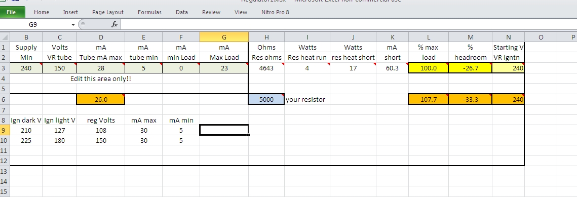
The easiest way to handle this is with a spreadsheet:
Spreadsheet download
Let’s say we have a rig with 280 volts no load voltage at maximum power
line, and 240 volts full load voltage at minimum power line voltage, and we
want to regulate a 6J5 oscillator. The 6J5 draws 23 mA worse case with the
worse crystal, and 0 mA when the key is open. (The VR tube has to unloaded
when it starts, or have to allow for that starting load.)
Keying Circuits
There are two primary types of old tube radio keying circuits, grid block
and cathode. While grid block is touted as the best, cathode keying can be
just as clean and safe. As a matter of fact, if you are willing to use a few
semiconductors, cathode keying can be easier to implement and much safer
than grid block!
Let’s look at what goes right and wrong with keying circuits.
Cathode Keying
Cathode keying is a form of self-bias control of tubes. The cathode is
lifted from ground, and floats up to a positive voltage above the grid’s
cutoff voltage required to pinch off anode and screen currents. The open key
voltage depends entirely on the negative grid biasing, in relationship to
the cathode’s positive voltage, required to cut the tube off. The positive
key voltage can be as low as a few volts, or as high as hundreds of volts,
with the same tubes!! I’ll show why that happens, and how to better
configure systems.
Tube Cutoff
In a tetrode or pentode, cutoff bias is heavily dependent on screen
voltage. Cutoff bias is almost independent of anode voltage, but cathode
open circuit voltage is highly dependent on screen voltage and
control grid voltages!
I plotted the following graph of a 6L6GC tube’s open circuit cathode
voltage:
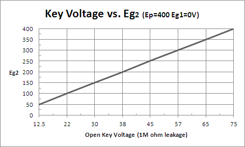
fig3
This shows a serious flaw in taking unregulated screen voltage through a
dropping resistor from a PA final amplifier anode supply. The screen voltage
will always rise to the anode supply voltage when the key is up. Obtaining
voltage from the anode supply without shunt clamping or shunt regulation
will severely increase either control grid negative bias for grid block or
oscillator keying, or increase cathode voltage across a cathode key.
Control grid voltage affects open-key voltage by increasing open key
voltage if positive to chassis, and decreasing open key voltage if negative.
The following graph shows open key voltage with screen voltage regulated at
200 volts, anode voltage of 400 volts, while grid bias is varied from -0 to
-80 volts:
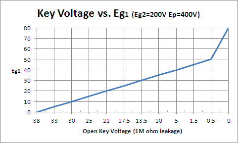
fig 4
Looking at a typical simple transmitter found on Internet and various
other places, we see circuits like this:
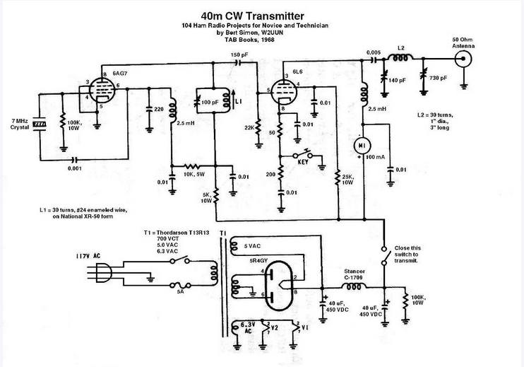
fig5
1.) Note the tube has no control grid bias. The required negative grid
voltage is derived entirely from rectification in the control grid-cathode
circuit. I’ll discuss the problem with this in detail later, but it is not a
good system. It is not good for loss of drive, it is not good for keyclicks,
and it is not good for cathode key voltage.
2.) Some self-bias without drive is obtained from a 50-ohm cathode
resistor, but again, it produces maximum bias when minimum bias is actually
required, and minimum bias when we want the tube cut off. The key filter, a
200 ohm resistor and .01 uF capacitor, has virtually no effect on
over-the-air clicks or bandwidth.
3.) The tube sources screen voltage from HV though a 25k resistor. Use of
a series resistor to a tube element, with no shunt load or regulation, works
fine in steady load conditions. It is a terrible method in any stage that
has greatly varying screen currents, because it does exactly the opposite of
what we want. This circuit, while simple, allows the screen voltage to rise
to full supply voltage whenever the key is up. While typical closed-key
screen voltage with proper tuning might be around 200 volts, open key screen
voltage would place the screen at full no-load plate voltage.
The method of using an open-ended series screen dropping resistor, along
with lack of fixed control grid bias, causes a radical increase in required
cut-off bias (open key voltage). Referring to the 6L6GC tube I
measured in figure 4,
we see a properly biased 6L6 tube would only require 10-20 volts of open key
voltage to cut off the transmitter. With the circuit above, since the screen
rises to ~400 volts, cathode open key voltage will be somewhere up around 75
volts.
The open key voltage of 75 volts further increases if the oscillator is
running, as in the circuit above, driving RF voltage to the final amplifier
grid. This happens because the tube’s grid acts like a detector anode, and
will pull the cathode well above the peak positive grid voltage plus the
original open key voltage, or at least above a portion of that original
voltage in addition to the grid drive voltage. Depending on oscillator peak
output at the PA grid, final amplifier open key voltage might easily exceed
100 volts.
Every time the key is closed, the key contacts have to discharge two .01
uF capacitors from a hundred volts to zero volts. While the 50 ohm cathode
resistor and 200 ohm dampening resistor reduce key spark, they key still has
to pull high voltages to ground. Making things worse, the screen has charged
its bypass to 400 volts. With the screen at 400 volts and control grid bias
at zero, key closure produces a very large leading edge power spike.
In the above transmitter measurement, RF envelope voltage (scaled from a
sample tap on a dummy load through an attenuator) decreases from 1.85 volts
peak to 1.43 volts, and .42 volt change. This represents a power change from
34.2 watts at the leading edge to 20.4 watts at the minimum during every
consecutive dot or dash. The significant key click energy, however, is
generated in the sharp leading and tailing edges of the envelope, not the
power overshoot. The leading edge just has more base power to generate
clicks.
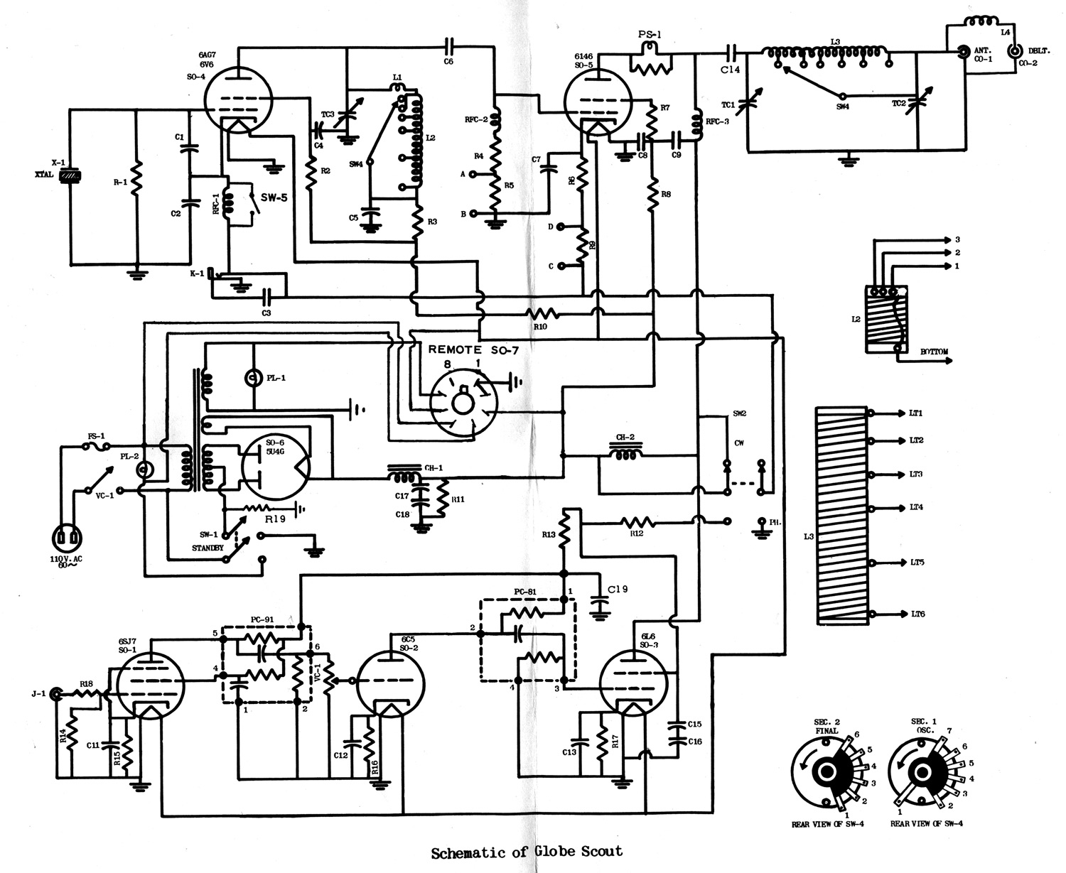
By the circuit below, we see the Globe Scout 65 design is not much
different. It is impossible to know who copied what, but all the mistakes
above mirror across the landscape of almost all early transmitters.
Surprisingly, it appears no dedicated attempt was made to add minimal parts
to clean up cathode-keyed transmitters. The only effort to improve operation
came in grid block systems.
Using Constant Current Characteristic Data
I thought, since I am designing a transmitter for myself, I would walk
through all the steps here.
First, I decided to eventually run a pair of 6146 tubes. I want to
measure the difference between 6146 tube types at HF, and document if they
really are as different as claimed. These tubes are also a good choice for
CW because they have high gain and are compact for the power level.
The 6146 data looks like:
|
Looking at tube characteristics we can pick a zero drive
bias point based on limiting plate dissipation at 20 watts with 700 volts
(20/700= .029 amps or 29 mA safe no-drive current). If we look below at the
-50 volt curve (just below G) we would have safe plate current with just
over -50 volts bias. This will eliminate any need for a screen clamp tube!
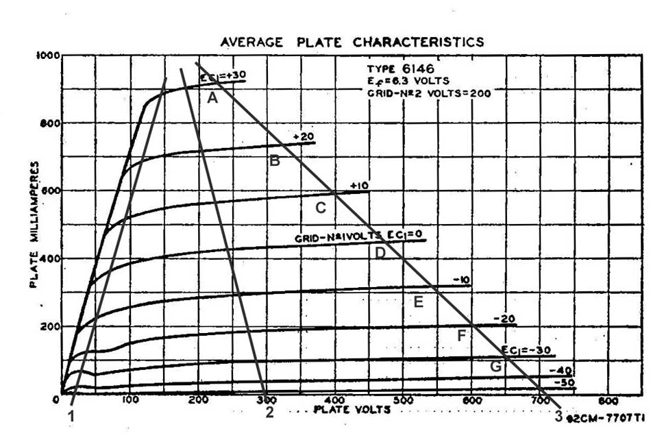
The rated output of a class-C 6146 at 700 volts is around 65 watts. This
would be with about 600 volts of peak anode voltage swing, or about 400
volts RMS voltage (because the waveform has high harmonic content, RMS
voltage swing is less than .707*peak we might expect).
At 130 watts for two tubes, the plate load impedance would be about 400^2
/ 130 = 1230 ohms. If we compare this estimate to the approximation Ep/2Ip=R
we have 700/.26*2 = 1346 ohms. I will design around my estimate of 1230 ohms
optimum plate load resistance. It is probably closer, although this value is
not critical.
Many articles suggest a network Q of 10-12, but in reality there is very
little difference in harmonic performance between a Q of 5-6, and a Q of
10-12.
The calculated difference in 2nd harmonic voltage going from a Q of ~7.5
to a Q of 12 is only 1.4 dB. If harmonics are an issue, it is more effective
to find other means to suppress them than to increase tank Q.
Good harmonic suppression is more a matter of construction and layout
than it is tank Q, so long as a somewhat reasonable Q is selected.
Minimum Q for a Pi-network is generally accepted to be 1+(sqrt of Rp/Rl).
This means if we plan for the highest impedance transformation we should be
OK at all other settings. If we don’t do that, the network might act
“spongy” or tune backwards, with less loading capacitance decreasing plate
current at dip.
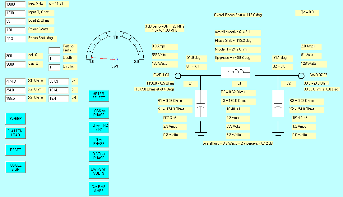
If we plan on a 1.5:1 load SWR, we should use sqrt of (1230/33) +1= 7.1.
Q would be 7.1. This also covers us at reduced power, because tank Q
increases at a faster rate than the required increase in Q as the ratio
becomes higher. We will never have a condition, at reduced power, where tank
Q is too low.
We will plan for a Q of 7.1 on all bands into 33 ohms (not 50 ohms). This
gives us headroom for SWR errors!!
Because of the large values required, 160-meter tank values determine the
physical area required for the tank circuit.
For proper headroom, we need just over 500 pF at 1kV for the plate tuning
capacitance. I decided to use a 208 pF capacitor with a 360 pF padding
capacitor for the plate. This will provide a tuning range of 375-568 pF on
160 meters. The tuning capacitor will need padded on 160 and 80 meters.
For loading, I have an 1100 pF air variable. The loading capacitor will
need padded only on 160.
| Band | Cp est | C pad | L | C load est | C pad |
| 160 | 507pF | 360pF | 16.4µH | 1100pF | 680pF |
| 80 | 261pF | 100pF | 8.4µH | 830pF | none |
| 40 | 130pF | none | 4.2µH | 415pF | none |
| 20 | 65pF | none | 2.1µH | 208pF | none |
| 15 | 44pF | none | 1.4µH | 138pF | none |
| 10 | 33pF | none | 0.7µH | 69pF | none |
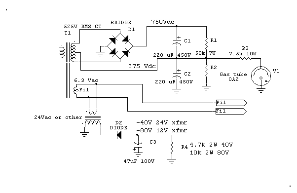
Power Supply
Also see this link
I’ve settled on a power supply. The schematic below is a
p-spice model of the supply. R5 and R6
actually represent internal resistance of the transformer. R1, R2, and R3
represent the load by external circuits, including voltage dividers and
vacuum tubes:
This supply moves the choke into the negative rectifier lead so I can
extract bias from the AC voltage appearing across the choke. I’ve done this
in a
Globe Scout and it works OK.
This is a full wave bridge that uses the transformer center tap to obtain
half voltage for the low level stages and screen grids of the PA tube. R1 is
the HV load, R2 the low voltage load, and R3 the bias system.
Diodes can be conventional 1N4007’s.
Here is how the real-world supply actually tested in a load-pull as R1
was varied. It looks like I have a good 100 watt supply, and a marginal 150
watt supply. This should be suitable for a single 6146B tube, or perhaps a
pair:
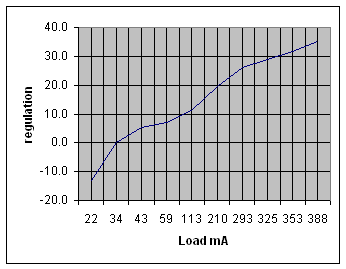
| 120 Vac Line |
With 50k bleeder across HV plus the additional load in left column. Current excludes bleeder. |
||||||||
| Load | P load | mA | HV | LV | bias neg | ESR | ERS2 | ESR3 | Sag % |
| 100000 | 6 | 8 | 758 | 298 | 180 | ||||
| 33000 | 16 | 22 | 722 | 307 | 230 | 2518 | -13.0 | ||
| 18500 | 21 | 34 | 628 | 317 | 325 | 7790 | 0.0 | ||
| 14000 | 25 | 43 | 596 | 319 | 335 | 3710 | 6089 | 5.4 | |
| 10000 | 34 | 59 | 587 | 313 | 345 | 558 | 1656 | 3666 | 7.0 |
| 5000 | 64 | 113 | 564 | 301 | 355 | 425 | 456 | 812 | 11.3 |
| 2500 | 111 | 210 | 526 | 280 | 400 | 389 | 402 | 417 | 19.4 |
| 1700 | 146 | 293 | 498 | 262 | 420 | 339 | 366 | 380 | 26.1 |
| 1500 | 158 | 325 | 487 | 255 | 435 | 347 | 341 | 363 | 29.0 |
| 1350 | 169 | 353 | 477 | 249 | 442 | 349 | 348 | 343 | 31.7 |
| 1200 | 180 | 388 | 465 | 240 | 450 | 351 | 350 | 349 | 35.1 |
Supply ESR looks to be around 350 ohms or so. I tried several chokes and
couldn’t find anything better, and no matter how reasonable bleeder current
or how much I increase inductance I can’t seem to get less than 700 volts no
load from my 700VCT transformer. I’m working on stabilizing the supply more
if possible.
Power Supplies
Power supplies are first, because everything depends on them. A transmitter’s
cleanliness and operating consistency can only be as good as the power supply
permits.
Old power supplies were often not that good. Most supplies used filter
chokes, which can be a very good thing with high vacuum rectifiers (reducing
peak current). Unfortunately, input chokes were often the wrong size for the
bleeder current, making regulation and peak currents worse than not even using a
choke! There is nothing worse than carefully following a recipe and seeking out
specific parts, just to have disastrous voltage regulation when done.
The primary advantage of a choke input filter is reduction of peak currents.
By virtue of energy storage and release, a properly-sized choke provides a
smoothly changing voltage boost throughout the low voltage part of the supply
sine wave. Conversely, the same choke provides a bucking voltage near peaks. The
mechanism behind this voltage bucking or boosting is an inductor’s tendency to readjust voltages
across the inductor as it tries to maintain constant current.
A properly sized input choke causes the rectifier to draw
current throughout the entire conduction period of the input cycle. This current
smoothing, almost appearing as a resistive load, extends in a closed loop from
power mains all the way through
the power transformer, rectifier system, and the first filter capacitor.
Capacitor input supplies can be very good for regulation, if high peak
currents are properly dealt with. The only significant operational
problems with higher power capacitor input supplies are caused by high peak currents,
even while average currents are about the same as a choke input supply. A
capacitor input supply draws all of the supply energy in a short period at the
rising edge and just over the crest of each power line cycle. These high peak currents cause abnormal heating
as they increase voltage drop in
components. Capacitor input supplies can be particularly tough on vacuum tubes,
and on old transformers using smaller copper sizes. To handle the apparent power
factor (APF) of heavy charging currents at the leading edge of each sine wave
voltage peak, capacitor input supplies
should use a little larger copper winding size. The capacitor input supply, in
essence, runs only on line voltage peaks. All load power is “taken off the
peaks”. This actually can flatten the peak of the line sine wave, causing
line voltage to measure almost normal on meters even while the mains are sagging
on peaks.
An example of a good power supply is in the AL1200 (AL12 series) power supplies.
I specifically designed the transformer for very tight coupling with minimal
flux leakage, and the largest possible copper size that would fit in the core
window. Because of the low ESR transformer, peak current is often limited just
by the ESR of the power mains. With a really stiff mains, the AL12 series will
hold voltage within 10% from no load to full load. The price for this voltage
stability is very high peak current. I’ve measured
about 40-50 amps peak current at the repeating line sine wave voltage crest leading
edges, while average current over the entire cycle is only about 12 amps. This
high peak-to-average current ratio clearly
calls for increased copper size throughout the primary system. Capacitor input
designs must minimize series resistance, or
regulation falls apart.
In comparison, a well-designed choke input supply (with properly sized choke) has an APF
(apparent power factor) of nearly unity. Current is drawn in smooth step with
voltage over the entire sine wave, even the descending slope of the waveform!
The smooth current window allows energy to be extracted from the mains over the
entire cycle. This allows much smaller copper sizes, since the choke input
supply requires far less attention to transformer and power line ESR
(equivalent series resistance). With a properly sized input choke and good
components, the power supply’s line loading appears as a pure resistance.
The bottom line on this is the user has two choices:
1.) Live with the high currents, while maintaining good life and good
regulation, by using low ESR (equivalent series resistance) transformers,
solid state rectifiers, and higher value filter capacitors2.) Use a properly designed choke input with higher ESR
components. “Properly Designed” being the key.